Circuit Topology of The vOICe

« The vOICe Home Page

This page defines the circuit topology of The vOICe hardware prototype (1989).

Circuit Topology (all top view) chip: INVCK 74LS04 hex inverters data: circuit clock, cristal controlled pin to pin to 1: 1A ALU5.13 14: VCC +5V 2: 1Y L2DAC.18 13: 6A XTAL.1 RX1.2 3: 2A DIVCK.13 12: 6Y CX.2 4: 2Y 5 L1SIN.11 L1FI.11 11: 5A CX.1 5: 3A 4 L3FI.11 DFF1.11 10: 5Y 9 XTAL.2 6: 3Y CNT1.13 L2FI.1 FI2.21 DFF2.3 9: 4A 10 RX2.1 7: GND GND 8: 4Y DIVCK.2 RX1.1 CX.2 RX1.2 INVCK.13 RX2.1 INVCK.9 RX2.2 CX.1 CX.1 RX2.2 INVCK.11 CX.2 RX1.1 INVCK.12 (XTAL=8MHz, RX1=RX2=510 ohm, CX=10nF) chip: DIVCK 74LS163 synchronous 4-bit binary counter data: divides circuit clock INVCK pin to pin to 1: CLEAR +5V 16: VCC +5V 2: CLOCK INVCK.8 15: CARRY OUT Not connected 3: A Not connected 14: QA Not connected 4: B Not connected 13: QB INVCK.3 5: C Not connected 12: QC Not connected 6: D Not connected 11: QD Not connected 7: ENABLE P 10 DFF2.9 10: ENABLE T 7 8: GND GND 9: LOAD +5V chip: CNT1 74LS393 dual 4-bit binary counter data: top counter, lsb's pin to pin to 1: 1A 8 14: VCC +5V 2: 1CLEAR GND 13: 2A INVCK.6 L1CNT.11 3: 1QA DFI1.6 L1CNT.18 12: 2CLEAR GND 4: 1QB DFI1.5 L1CNT.17 11: 2QA L1CNT.3 5: 1QC Not connected 10: 2QB L1CNT.4 6: 1QD CNT2.13 9: 2QC L1CNT.7 7: GND GND 8: 2QD L1CNT.8 1 chip: CNT2 74LS393 dual 4-bit binary counter data: middle counter pin to pin to 1: 1A 8 14: VCC +5V 2: 1CLEAR GND 13: 2A CNT1.6 MUX.2 3: 1QA Not connected 12: 2CLEAR GND 4: 1QB Not connected 11: 2QA Not connected 5: 1QC SW.1 10: 2QB Not connected 6: 1QD SW.3 9: 2QC Not connected 7: GND GND 8: 2QD 1 SW.1 CNT2.5 SW.2 MUX.3 SW.3 CNT2.6 (SW=tumble switch: either SW.1 and SW.2 or SW.2 and SW.3 shorted) chip: CNT3 74LS393 dual 4-bit binary counter data: bottom counter, msb's pin to pin to 1: 1A 8 14: VCC +5V 2: 1CLEAR GND 13: 2A MUX.4 3: 1QA L2CNT.18 12: 2CLEAR GND 4: 1QB L2CNT.17 11: 2QA L2CNT.3 5: 1QC L2CNT.14 10: 2QB L2CNT.4 6: 1QD Not connected 9: 2QC L2CNT.7 7: GND GND 8: 2QD L2CNT.8 1 chip: L1CNT 74LS374 octal D-type edge-triggered flip-flops with 3-state data: top latch for addresses from counters CNT, lsb's pin to pin to 1: OUTPUT CTRL GND 20: VCC +5V 2: 1Q FI1.8 19: 8Q FI1.4 3: 1D CNT1.11 DFI1.10 18: 8D CNT1.3 4: 2D CNT1.10 DFI1.9 17: 7D CNT1.4 5: 2Q FI1.7 16: 7Q FI1.3 DFF1.12 6: 3Q FI1.6 15: 6Q Not connected 7: 3D CNT1.9 DFI1.8 14: 6D Not connected 8: 4D CNT1.8 DFI1.7 13: 5D Not connected 9: 4Q FI1.5 12: 5Q Not connected 10: GND GND 11: CLOCK CNT1.13 L2CNT.11 chip: L2CNT 74LS374 octal D-type edge-triggered flip-flops with 3-state data: bottom latch for addresses from counters CNT, msb's pin to pin to 1: OUTPUT CTRL GND 20: VCC +5V 2: 1Q PIX4.1 19: 8Q DMX.2 3: 1D CNT3.11 18: 8D CNT3.3 4: 2D CNT3.10 17: 7D CNT3.4 5: 2Q PIX4.17 16: 7Q DMX.3 6: 3Q PIX4.16 15: 6Q OR.10 7: 3D CNT3.9 14: 6D CNT3.5 8: 4D CNT3.8 13: 5D Not connected 9: 4Q PIX4.15 12: 5Q Not connected 10: GND GND 11: CLOCK L1CNT.11 OR.13 chip: DFI1 27128 16Kx8 EPROM, 250ns data: dfidat.lsb, top EPROM pin to pin to 1: VPP +5V 28: VCC +5V 2: A12 +5V 27: PGM +5V 3: A7 +5V 26: A13 +5V 4: A6 +5V 25: A8 +5V 5: A5 CNT1.4 DFI2.5 24: A9 +5V 6: A4 CNT1.3 DFI2.6 23: A11 +5V 7: A3 L1CNT.8 DFI2.7 22: G GND 8: A2 L1CNT.7 DFI2.8 21: A10 +5V 9: A1 L1CNT.4 DFI2.9 20: E GND 10: A0 L1CNT.3 DFI2.10 19: Q8 AD2.11 11: Q1 AD1.6 18: Q7 AD2.15 12: Q2 AD1.2 17: Q6 AD2.2 13: Q3 AD1.15 16: Q5 AD2.6 14: GND GND 15: Q4 AD1.11 chip: DFI2 27128 16Kx8 EPROM, 250ns data: dfidat.msb, bottom EPROM pin to pin to 1: VPP +5V 28: VCC +5V 2: A12 +5V 27: PGM +5V 3: A7 +5V 26: A13 +5V 4: A6 +5V 25: A8 +5V 5: A5 DFI1.5 24: A9 +5V 6: A4 DFI1.6 23: A11 +5V 7: A3 DFI1.7 22: G GND 8: A2 DFI1.8 21: A10 +5V 9: A1 DFI1.9 20: E GND 10: A0 DFI1.10 19: Q8 AD4.11 11: Q1 AD3.6 18: Q7 AD4.15 12: Q2 AD3.2 17: Q6 AD4.2 13: Q3 AD3.15 16: Q5 AD4.6 14: GND GND 15: Q4 AD3.11 chip: FI1 6116 2Kx8 SRAM, 150ns data: fi storage, top SRAM, lsb's pin to pin to 1: A7 +5V 24: VCC +5V 2: A6 +5V 23: A8 +5V 3: A5 L1CNT.16 FI2.3 22: A9 +5V 4: A4 L1CNT.19 FI2.4 21: WE FI2.21 5: A3 L1CNT.9 FI2.5 20: OE GND 6: A2 L1CNT.6 FI2.6 19: A10 +5V 7: A1 L1CNT.5 FI2.7 18: CS GND 8: A0 L1CNT.2 FI2.8 17: I/O8 AD2.12 9: I/O1 AD1.5 16: I/O7 AD2.14 10: I/O2 AD1.3 15: I/O6 AD2.3 11: I/O3 AD1.14 14: I/O5 AD2.5 12: GND GND 13: I/O4 AD1.12 chip: FI2 6116 2Kx8 SRAM, 150ns data: fi storage, bottom SRAM, msb's pin to pin to 1: A7 +5V 24: VCC +5V 2: A6 +5V 23: A8 +5V 3: A5 FI1.3 PIX4.2 22: A9 +5V 4: A4 FI1.4 PIX4.3 21: WE INVCK.6 FI1.21 5: A3 FI1.5 PIX4.4 20: OE GND 6: A2 FI1.6 PIX4.7 19: A10 +5V 7: A1 FI1.7 PIX4.6 18: CS GND 8: A0 FI1.8 PIX4.5 17: I/O8 AD4.12 9: I/O1 AD3.5 16: I/O7 AD4.14 10: I/O2 AD3.3 15: I/O6 AD4.3 11: I/O3 AD3.14 14: I/O5 AD4.5 12: GND GND 13: I/O4 AD3.12 chip: L1FI 74LS374 octal D-type edge-triggered flip-flops with 3-state data: latch for addition of fi and dfi, lsb's pin to pin to 1: OUTPUT CTRL L2FI.1 20: VCC +5V 2: 1Q AD2.12 19: 8Q AD2.3 3: 1D AD2.10 L3FI.3 18: 8D AD2.1 L3FI.18 4: 2D AD2.13 L3FI.4 17: 7D AD2.4 L3FI.17 5: 2Q AD2.14 16: 7Q AD2.5 6: 3Q AD1.12 15: 6Q AD1.3 7: 3D AD1.10 14: 6D AD1.1 8: 4D AD1.13 13: 5D AD1.4 9: 4Q AD1.14 12: 5Q AD1.5 10: GND GND 11: CLOCK INVCK.4 L2FI.11 chip: L2FI 74LS374 octal D-type edge-triggered flip-flops with 3-state data: latch for addition of fi and dfi, msb's pin to pin to 1: OUTPUT CTRL INVCK.6 L1FI.1 XOR3.12 20: VCC +5V 2: 1Q AD4.12 19: 8Q AD4.3 3: 1D AD4.10 L4FI.3 18: 8D AD4.1 L4FI.18 4: 2D AD4.13 L4FI.4 17: 7D AD4.4 L4FI.17 5: 2Q AD4.14 16: 7Q AD4.5 6: 3Q AD3.12 15: 6Q AD3.3 7: 3D AD3.10 L4FI.7 14: 6D AD3.1 L4FI.14 8: 4D AD3.13 L4FI.8 13: 5D AD3.4 L4FI.13 9: 4Q AD3.14 12: 5Q AD3.5 10: GND GND 11: CLOCK L1FI.11 chip: AD1 74LS283 4-bit binary full adders data: adds fi and dfi, lsb's pin to pin to 1: S2 L1FI.14 16: VCC +5V 2: B2 DFI1.12 15: B3 DFI1.13 3: A2 FI1.10 L1FI.15 14: A3 FI1.11 L1FI.9 4: S1 L1FI.13 13: S3 L1FI.8 5: A1 FI1.9 L1FI.12 12: A4 FI1.13 L1FI.6 6: B1 DFI1.11 11: B4 DFI1.15 7: C0 GND 10: S4 L1FI.7 8: GND GND 9: C4 AD2.7 chip: AD2 74LS283 4-bit binary full adders data: adds fi and dfi pin to pin to 1: S2 L1FI.18 16: VCC +5V 2: B2 DFI1.17 15: B3 DFI1.18 3: A2 FI1.15 L1FI.19 14: A3 FI1.16 L1FI.5 4: S1 L1FI.17 13: S3 L1FI.4 5: A1 FI1.14 L1FI.16 12: A4 FI1.17 L1FI.2 6: B1 DFI1.16 11: B4 DFI1.19 7: C0 AD1.9 10: S4 L1FI.3 8: GND GND 9: C4 AD3.7 chip: AD3 74LS283 4-bit binary full adders data: adds fi and dfi pin to pin to 1: S2 L2FI.14 16: VCC +5V 2: B2 DFI2.12 15: B3 DFI2.13 3: A2 FI2.10 L2FI.15 14: A3 FI2.11 L2FI.9 4: S1 L2FI.13 13: S3 L2FI.8 5: A1 FI2.9 L2FI.12 12: A4 FI2.13 L2FI.6 6: B1 DFI2.11 11: B4 DFI2.15 7: C0 AD2.9 10: S4 L2FI.7 8: GND GND 9: C4 AD4.7 chip: AD4 74LS283 4-bit binary full adders data: adds fi and dfi, msb's pin to pin to 1: S2 L2FI.18 16: VCC +5V 2: B2 DFI2.17 15: B3 DFI2.18 3: A2 FI2.15 L2FI.19 14: A3 FI2.16 L2FI.5 4: S1 L2FI.17 13: S3 L2FI.4 5: A1 FI2.14 L2FI.16 12: A4 FI2.17 L2FI.2 6: B1 DFI2.16 11: B4 DFI2.19 7: C0 AD3.9 10: S4 L2FI.3 8: GND GND 9: C4 Not connected chip: L3FI 74LS374 octal D-type edge-triggered flip-flops with 3-state data: latch for shifting fi to XOR, lsb's pin to pin to 1: OUTPUT CTRL GND 20: VCC +5V 2: 1Q XOR1.1 19: 8Q XOR1.13 3: 1D L1FI.3 18: 8D L1FI.18 4: 2D L1FI.4 17: 7D L1FI.17 5: 2Q XOR1.6 16: 7Q XOR1.8 6: 3Q SIN2.26 15: 6Q SIN2.23 7: 3D PIX4.11 14: 6D PIX4.13 8: 4D PIX4.12 13: 5D PIX4.14 9: 4Q SIN2.2 12: 5Q SIN2.21 10: GND GND 11: CLOCK INVCK.5 L4FI.11 chip: L4FI 74LS374 octal D-type edge-triggered flip-flops with 3-state data: latch for shifting fi to XOR, msb's pin to pin to 1: OUTPUT CTRL GND 20: VCC +5V 2: 1Q DFF2.2 19: 8Q XOR3.6 3: 1D L2FI.3 18: 8D L2FI.18 4: 2D L2FI.4 17: 7D L2FI.17 5: 2Q XOR3.9 16: 7Q XOR3.8 6: 3Q XOR2.1 15: 6Q XOR2.13 7: 3D L2FI.7 14: 6D L2FI.14 8: 4D L2FI.8 13: 5D L2FI.13 9: 4Q XOR2.6 12: 5Q XOR2.8 10: GND GND 11: CLOCK L3FI.11 chip: XOR1 74LS386 quad 2-input exclusive-or gates data: can invert fi, lsb's pin to pin to 1: 1A L3FI.2 14: VCC +5V 2: 1B 12 XOR2.5 13: 4B L3FI.19 3: 1Y SIN2.7 12: 4A 9 2 4: 2Y SIN2.8 11: 4Y SIN2.10 5: 2A 9 10: 3Y SIN2.9 6: 2B L3FI.5 9: 3B 5 12 7: GND GND 8: 3A L3FI.16 chip: XOR2 74LS386 quad 2-input exclusive-or gates data: can invert fi, middle bits pin to pin to 1: 1A L4FI.6 14: VCC +5V 2: 1B 12 XOR3.5 13: 4B L4FI.15 3: 1Y SIN2.3 12: 4A 9 2 4: 2Y SIN2.4 11: 4Y SIN2.5 5: 2A XOR1.2 9 10: 3Y SIN2.6 6: 2B L4FI.9 9: 3B 5 12 7: GND GND 8: 3A L4FI.12 chip: XOR3 74LS386 quad 2-input exclusive-or gates data: can invert fi, msb's pin to pin to 1: 1A Not connected 14: VCC +5V 2: 1B Not connected 13: 4B INV1.11 3: 1Y Not connected 12: 4A L2FI.1 4: 2Y SIN2.24 11: 4Y SAM.13 5: 2A XOR2.2 9 10: 3Y SIN2.25 6: 2B L4FI.19 9: 3B L4FI.5 5 7: GND GND 8: 3A L4FI.16 chip: SIN1 27128 16Kx8 EPROM, 250ns data: sindat.lsb, right EPROM pin to pin to 1: VPP +5V 28: VCC +5V 2: A12 SIN2.2 27: PGM +5V 3: A7 SIN2.3 26: A13 SIN2.26 4: A6 SIN2.4 25: A8 SIN2.25 5: A5 SIN2.5 24: A9 SIN2.24 6: A4 SIN2.6 23: A11 SIN2.23 7: A3 SIN2.7 22: G GND 8: A2 SIN2.8 21: A10 SIN2.21 9: A1 SIN2.9 20: E GND 10: A0 SIN2.10 19: Q8 ALU2.18 11: Q1 ALU1.1 18: Q7 ALU2.20 12: Q2 ALU1.22 17: Q6 ALU2.22 13: Q3 ALU1.20 16: Q5 ALU2.1 14: GND GND 15: Q4 ALU1.18 chip: SIN2 27128 16Kx8 EPROM, 250ns data: sindat.msb, left EPROM pin to pin to 1: VPP +5V 28: VCC +5V 2: A12 L3FI.9 SIN1.2 27: PGM +5V 3: A7 XOR2.3 SIN1.3 26: A13 L3FI.6 SIN1.26 4: A6 XOR2.4 SIN1.4 25: A8 XOR3.10 SIN1.25 5: A5 XOR2.11 SIN1.5 24: A9 XOR3.4 SIN1.24 6: A4 XOR2.10 SIN1.6 23: A11 L3FI.15 SIN1.23 7: A3 XOR1.3 SIN1.7 22: G GND 8: A2 XOR1.4 SIN1.8 21: A10 L3FI.12 SIN1.21 9: A1 XOR1.10 SIN1.9 20: E GND 10: A0 XOR1.11 SIN1.10 19: Q8 ALU4.18 11: Q1 ALU3.1 18: Q7 ALU4.20 12: Q2 ALU3.22 17: Q6 ALU4.22 13: Q3 ALU3.20 16: Q5 ALU4.1 14: GND GND 15: Q4 ALU3.18 chip: L1SIN 74LS273 octal D-type edge-triggered flip-flops with clear data: latch for addition of sine values, lsb's pin to pin to 1: CLEAR L2SIN.1 INV1.4 20: VCC +5V 2: 1Q ALU1.19 19: 8Q ALU1.23 3: 1D ALU1.13 18: 8D ALU1.10 4: 2D ALU1.11 17: 7D ALU1.9 5: 2Q ALU1.21 16: 7Q ALU1.2 6: 3Q Not connected 15: 6Q Not connected 7: 3D Not connected 14: 6D Not connected 8: 4D Not connected 13: 5D Not connected 9: 4Q Not connected 12: 5Q Not connected 10: GND GND 11: CLOCK INVCK.4 L2SIN.11 chip: L2SIN 74LS273 octal D-type edge-triggered flip-flops with clear data: latch for addition of sine values pin to pin to 1: CLEAR L3SIN.1 L1SIN.1 20: VCC +5V 2: 1Q ALU3.19 19: 8Q ALU3.23 3: 1D ALU3.13 18: 8D ALU3.10 4: 2D ALU3.11 17: 7D ALU3.9 5: 2Q ALU3.21 16: 7Q ALU3.2 6: 3Q ALU2.19 15: 6Q ALU2.23 7: 3D ALU2.13 14: 6D ALU2.10 8: 4D ALU2.11 13: 5D ALU2.9 9: 4Q ALU2.21 12: 5Q ALU2.2 10: GND GND 11: CLOCK L1SIN.11 L3SIN.11 chip: L3SIN 74LS273 octal D-type edge-triggered flip-flops with clear data: latch for addition of sine values, msb's pin to pin to 1: CLEAR L2SIN.1 20: VCC +5V 2: 1Q ALU5.19 19: 8Q ALU5.23 3: 1D ALU5.13 18: 8D ALU5.10 4: 2D ALU5.11 17: 7D ALU5.9 5: 2Q ALU5.21 16: 7Q ALU5.2 6: 3Q ALU4.19 15: 6Q ALU4.23 7: 3D ALU4.13 14: 6D ALU4.10 8: 4D ALU4.11 13: 5D ALU4.9 9: 4Q ALU4.21 12: 5Q ALU4.2 10: GND GND 11: CLOCK L2SIN.11 chip: ALU1 74LS181 ALU/function generator, active high data data: add/subtract sine values, lsb's pin to pin to 1: B0 SIN1.11 24: VCC +5V 2: A0 L1SIN.16 23: A1 L1SIN.19 3: S3 6 7 22: B1 SIN1.12 4: S2 5 ALU2.4 21: A2 L1SIN.5 5: S1 4 20: B2 SIN1.13 6: S0 3 19: A3 L1SIN.2 7: Cn 3 ALU2.6 18: B3 SIN1.15 8: M GND 17: Y Not connected 9: F0 L1SIN.17 16: Cn+4 ALU2.7 10: F1 L1SIN.18 15: X Not connected 11: F2 L1SIN.4 14: A=B Not connected 12: GND GND 13: F3 L1SIN.3 chip: ALU2 74LS181 ALU/function generator, active high data data: add/subtract sine values pin to pin to 1: B0 SIN1.16 24: VCC +5V 2: A0 L2SIN.12 23: A1 L2SIN.15 3: S3 6 ALU3.6 22: B1 SIN1.17 4: S2 5 ALU1.4 ALU3.4 21: A2 L2SIN.9 5: S1 4 20: B2 SIN1.18 6: S0 3 ALU1.7 19: A3 L2SIN.6 7: Cn ALU1.16 18: B3 SIN1.19 8: M GND 17: Y Not connected 9: F0 L2SIN.13 L2DAC.17 16: Cn+4 ALU3.7 10: F1 L2SIN.14 L1DAC.7 15: X Not connected 11: F2 L2SIN.8 L1DAC.8 14: A=B Not connected 12: GND GND 13: F3 L2SIN.7 L1DAC.14 chip: ALU3 74LS181 ALU/function generator, active high data data: add/subtract sine values pin to pin to 1: B0 SIN2.11 24: VCC +5V 2: A0 L2SIN.16 23: A1 L2SIN.19 3: S3 6 ALU4.6 22: B1 SIN2.12 4: S2 5 ALU2.4 ALU4.4 21: A2 L2SIN.5 5: S1 4 20: B2 SIN2.13 6: S0 3 ALU2.3 19: A3 L2SIN.2 7: Cn ALU2.16 18: B3 SIN2.15 8: M GND 17: Y Not connected 9: F0 L2SIN.17 L1DAC.13 16: Cn+4 ALU4.7 10: F1 L2SIN.18 L1DAC.3 15: X Not connected 11: F2 L2SIN.4 L1DAC.4 14: A=B Not connected 12: GND GND 13: F3 L2SIN.3 L1DAC.18 chip: ALU4 74LS181 ALU/function generator, active high data data: add/subtract sine values pin to pin to 1: B0 SIN2.16 24: VCC +5V 2: A0 L3SIN.12 23: A1 L3SIN.15 3: S3 6 ALU5.6 22: B1 SIN2.17 4: S2 5 ALU3.4 ALU5.4 21: A2 L3SIN.9 5: S1 4 20: B2 SIN2.18 6: S0 3 ALU3.3 19: A3 L3SIN.6 7: Cn ALU3.16 18: B3 SIN2.19 8: M GND 17: Y Not connected 9: F0 L3SIN.13 L1DAC.17 16: Cn+4 ALU5.7 10: F1 L3SIN.14 L2DAC.7 15: X Not connected 11: F2 L3SIN.8 L2DAC.8 14: A=B Not connected 12: GND GND 13: F3 L3SIN.7 L2DAC.14 chip: ALU5 74LS181 ALU/function generator, active high data data: add/subtract sine values, msb's pin to pin to 1: B0 GND 24: VCC +5V 2: A0 L3SIN.16 23: A1 L3SIN.19 3: S3 6 DFF2.6 22: B1 GND 4: S2 5 ALU4.4 21: A2 L3SIN.5 5: S1 4 DFF2.5 20: B2 GND 6: S0 3 ALU4.3 19: A3 L3SIN.2 7: Cn ALU4.16 18: B3 GND 8: M GND 17: Y Not connected 9: F0 L3SIN.17 L2DAC.13 16: Cn+4 Not connected 10: F1 L3SIN.18 L2DAC.3 15: X Not connected 11: F2 L3SIN.4 L2DAC.4 14: A=B Not connected 12: GND GND 13: F3 L3SIN.3 INVCK.1 chip: L1DAC 74LS374 octal D-type edge-triggered flip-flops with 3-state data: latch for shifting signal to DAC, lsb's pin to pin to 1: OUTPUT CTRL GND 20: VCC +5V 2: 1Q DAC.12 19: 8Q DAC.10 3: 1D ALU3.10 18: 8D ALU3.13 4: 2D ALU3.11 17: 7D ALU4.9 5: 2Q DAC.11 16: 7Q DAC.9 6: 3Q DAC.16 15: 6Q DAC.14 7: 3D ALU2.10 14: 6D ALU2.13 8: 4D ALU2.11 13: 5D ALU3.9 9: 4Q DAC.15 12: 5Q DAC.13 10: GND GND 11: CLOCK L2DAC.11 INV1.3 NOR4.10 chip: L2DAC 74LS374 octal D-type edge-triggered flip-flops with 3-state data: latch for shifting signal to DAC, msb's pin to pin to 1: OUTPUT CTRL GND 20: VCC +5V 2: 1Q DAC.4 19: 8Q DAC.2 3: 1D ALU5.10 18: 8D INVCK.2 4: 2D ALU5.11 17: 7D ALU2.9 5: 2Q DAC.3 16: 7Q DAC.17 6: 3Q DAC.8 15: 6Q DAC.6 7: 3D ALU4.10 14: 6D ALU4.13 8: 4D ALU4.11 13: 5D ALU5.9 9: 4Q DAC.7 12: 5Q DAC.5 10: GND GND chip: DAC AD7546 16-bit multiplying DA-converter data: pin to pin to 1: NC GND 40: VDD +12V 2: DB15 L2DAC.19 39: NC GND 3: DB14 L2DAC.5 38: NC GND 4: DB13 L2DAC.2 37: VREF+ +5V 5: DB12 L2DAC.12 36: R1 GND 6: DB11 L2DAC.15 35: R2 GND 7: DB10 L2DAC.9 34: VREF- GND 8: DB9 L2DAC.6 33: A1OUT AMP1.1 9: DB8 L1DAC.16 32: A1- AMP1.2 10: DB7 L1DAC.19 31: A1+ AMP1.3 11: DB6 L1DAC.5 30: NC GND 12: DB5 L1DAC.2 29: A2OUT AMP1.7 13: DB4 L1DAC.12 28: A2- AMP1.6 14: DB3 L1DAC.15 27: A2+ AMP1.5 15: DB2 L1DAC.9 26: NC GND 16: DB1 L1DAC.6 25: VOUT AMP2.3 17: DB0 L2DAC.16 24: SW1 AMP2.1 18: CS GND 23: NC GND 19: WR DFF1.9 22: SW2 AMP2.5 CH.1 20: DGND GND 21: VSS GND CH.1 DAC.22 CH.2 GND (CH=10nF deglitcher) chip: AMP1 AD644JH dual high speed implanted FET-input opamp data: buffer amplifiers for DAC pin to pin to 1: 1OUTPUT DAC.33 8: V+ +12V 2: 1INPUT- DAC.32 7: 2OUTPUT DAC.29 3: 1INPUT+ DAC.31 6: 2INPUT- DAC.28 4: V- -12V 5: 2INPUT+ DAC.27 chip: AMP2 TL084 quad opamps data: output of DAC to headphones pin to pin to 1: 1OUTPUT 2 DAC.24 14: 4OUTPUT 13 RO3.1 2: 1INPUT- 1 13: 4INPUT- 14 3: 1INPUT+ DAC.25 12: 4INPUT+ DAC.22 4: V+ +12V 11: V- -12V 5: 2INPUT+ 10 10: 3INPUT+ 5 RO5.2 6: 2INPUT- RO2.1 CO2.1 RO1.1 9: 3INPUT- POT3.2 RO4.1 (CO4.1) 7: 2OUTPUT RO2.2 CO2.2 CO3.1 8: 3OUTPUT RO4.2 (CO4.2) CO1.2 The reason for brackets around CO4 lies in a later minor modification: CO4.2 has been disconnected, just to have a non-attenuated tap on the output signal for making spectrograms. With the capacitor, there was a noticeable diminuation at the higher system frequencies, which led to loss of significant bits in and complicated rescalings for the 8-bit sound-samplings (DeLuxe sound sampler). The system performance changes very little from the viewpoint of perception. Action: Januari 14, 1990. The extra tap now has a 100nF coupling capacitor connected to AMP2.8. The other terminal of this capacitor leads to the sound sampler input. RO1.1 AMP2.6 RO1.2 CO1.1 CO1.1 RO1.2 CO1.2 AMP2.8 RO2.1 AMP2.6 RO2.2 AMP2.7 CO2.1 AMP2.6 CO2.2 AMP2.7 CO3.1 AMP2.7 CO3.2 PHONE.1 PHONE.1 CO3.2 PHONE.2 GND (RO1=RO2=10K, CO1=1uF, CO2=10nF, CO3=470uF, PHONE=Headphones 32 ohm) RO3.1 AMP2.14 RO3.2 POT3.1 RO4.1 AMP2.9 RO4.2 AMP2.8 CO4.1 AMP2.9 CO4.2 AMP2.8 RO5.1 +5V RO5.2 RO6.1 AMP2.10 RO6.1 RO5.2 RO6.2 GND POT3.1 RO3.2 POT3.2 AMP2.9 POT3.3 Not connected (fixed contact) (RO3=RO4=10K, RO5=RO6=2K2, CO3=10nF, POT3=100K potmeter) chip: AMP3 TL084 quad opamps data: sample and hold amplifiers pin to pin to 1: 1OUTPUT Not connected 14: 4OUTPUT Not connected 2: 1INPUT- Not connected 13: 4INPUT- Not connected 3: 1INPUT+ Not connected 12: 4INPUT+ Not connected 4: V+ +12V 11: V- -12V 5: 2INPUT+ SAM.2 CS.1 10: 3INPUT+ RI.1 6: 2INPUT- 7 9: 3INPUT- 8 7: 2OUTPUT 6 ADC1.2 8: 3OUTPUT 9 SAM.1 CS.1 AMP3.5 CS.2 GND (CS=33pF hold-capacitor) chip: NOR1 74LS02 quad 2-input nor-gates data: random logic, top chip pin to pin to 1: 1Y NOR2.8 INV1.11 14: VCC +5V 2: 1A NOR2.13 13: 4Y NOR1.6 3: 1B OR.6 NOR2.12 12: 4B NOR1.4 4: 2Y NOR1.12 NOR1.9 11: 4A NOR1.10 5: 2A NOR1.8 10: 3Y NOR1.11 INV1.9 6: 2B NOR1.13 9: 3B NOR1.4 7: GND GND 8: 3A NOR1.5 MUX.1 chip: NOR2 74LS02 quad 2-input nor-gates data: random logic pin to pin to 1: 1Y NOR3.8 14: VCC +5V 2: 1A NOR3.10 13: 4Y NOR1.2 NOR2.9 3: 1B NOR2.4 12: 4B NOR1.3 4: 2Y NOR2.3 INV1.13 11: 4A NOR2.10 5: 2A NOR3.10 10: 3Y NOR2.11 6: 2B OR.8 NOR3.9 9: 3B NOR2.13 7: GND GND 8: 3A NOR1.1 chip: NOR3 74LS02 quad 2-input nor-gates data: random logic pin to pin to 1: 1Y NOR3.5 NOR3.12 14: VCC +5V 2: 1A NOR3.11 13: 4Y NOR3.6 INV1.5 3: 1B NOR3.4 12: 4B NOR3.1 4: 2Y NOR3.3 11: 4A NOR3.2 MON.13 5: 2A NOR3.1 10: 3Y NOR2.2 NOR2.5 6: 2B NOR3.13 9: 3B NOR2.6 7: GND GND 8: 3A NOR2.1 chip: NOR4 74LS02 quad 2-input nor-gates data: random logic, bottom chip pin to pin to 1: 1Y Not connected 14: VCC +5V 2: 1A Not connected 13: 4Y NOR4.6 3: 1B Not connected 12: 4B NOR4.4 4: 2Y NOR4.9 NOR4.12 11: 4A NOR4.10 5: 2A NOR4.8 10: 3Y NOR4.11 L1DAC.11 6: 2B NOR4.13 9: 3B NOR4.4 7: GND GND 8: 3A NOR4.5 DFF1.9 chip: DFF1 74LS74 dual D-type flip-flops with preset and clear data: random logic, top chip pin to pin to 1: 1CLR INV1.8 14: VCC +5V 2: 1D +5V 13: 2CLR +5V 3: 1CK +5V 12: 2D L1CNT.16 OR.9 4: 1PR INV1.6 11: 2CK INVCK.5 5: 1Q Not connected 10: 2PR +5V 6: 1Q OR.5 9: 2Q DAC.19 NOR4.8 7: GND GND 8: 2Q Not connected chip: OR 74LS32 quad 2-input or-gates data: random logic pin to pin to 1: 1A Not connected 14: VCC +5V 2: 1B Not connected 13: 4B L2CNT.11 3: 1Y Not connected 12: 4A OR.10 MUX.1 4: 2A MON.5 11: 4Y LADC.1 PIX1.10 5: 2B DFF1.6 10: 3B OR.12 L2CNT.15 6: 2Y NOR1.3 9: 3A DFF1.12 7: GND GND 8: 3Y NOR2.6 chip: DFF2 74LS74 dual D-type flip-flops with preset and clear data: random logic, bottom chip pin to pin to 1: 1CLR +5V 14: VCC +5V 2: 1D L4FI.2 13: 2CLR INV1.12 3: 1CK INVCK.6 12: 2D +5V 4: 1PR +5V 11: 2CK +5V 5: 1Q ALU5.5 10: 2PR INV1.10 6: 1Q ALU5.3 9: 2Q DIVCK.7 7: GND GND 8: 2Q Not connected chip: INV1 74LS04 hex inverters data: random logic pin to pin to 1: 1A Not connected 14: VCC +5V 2: 1Y Not connected 13: 6A NOR2.4 3: 2A L1DAC.11 12: 6Y DFF2.13 4: 2Y L1SIN.1 11: 5A NOR1.1 XOR3.13 5: 3A NOR3.13 10: 5Y DFF2.10 6: 3Y DFF1.4 9: 4A NOR1.10 7: GND GND 8: 4Y DFF1.1 chip: MON 74LS221 dual monostable multivibrators data: delays sync-pulses video signal 1.52ms and 15.2us pin to pin to 1: 1A GND 16: VCC +5V 2: 1B ADVSNC.7 15: 1Rext/Cext CM1.2 RM1.1 3: 1CLR +5V 14: Cext CM1.1 4: 1Q Not connected 13: 1Q NOR3.11 5: 2Q OR.4 12: 2Q Not connected 6: 2Cext CM2.1 11: 2CLR +5V 7: 2Rext/Cext CM2.2 RM2.1 10: 2B ADHSNC.7 8: GND GND 9: 2A GND RM1.1 MON.15 RM1.2 +5V CM1.1 MON.14 CM1.2 MON.15 RM2.1 MON.7 RM2.2 +5V CM2.1 MON.6 CM2.2 MON.7 (RM1=10K, CM1=0.22uF, RM2=2.7K, CM2=10nF) chip: SAM 4066B CMOS quad analog switches data: sample-and-hold switch for video input pin to pin to 1: In1 AMP3.8 14: VDD +5V 2: Out1 AMP3.5 13: Control1 XOR3.11 LADC.11 3: Out2 GND 12: Control4 GND 4: In2 GND 11: In4 GND 5: Control2 GND 10: Out4 GND 6: Control3 GND 9: Out3 GND 7: VSS GND 8: In3 GND chip: LADC 74LS374 octal D-type edge-triggered flip-flops with 3-state data: latch for video SRAM pin to pin to 1: OUTPUT CTRL OR.11 20: VCC +5V 2: 1Q Not connected 19: 8Q Not connected 3: 1D Not connected 18: 8D Not connected 4: 2D Not connected 17: 7D Not connected 5: 2Q Not connected 16: 7Q Not connected 6: 3Q PIX1.11 15: 6Q PIX1.13 7: 3D INV2.12 14: 6D NAND2.8 8: 4D INV2.2 13: 5D N4AND.6 9: 4Q PIX1.12 12: 5Q PIX1.14 10: GND GND 11: CLOCK SAM.13 chip: INV2 74LS04 hex inverters data: random logic pin to pin to 1: 1A NAND2.6 14: VCC +5V 2: 1Y LADC.8 13: 6A ADC8.7 3: 2A Not connected 12: 6Y LADC.7 4: 2Y Not connected 11: 5A Not connected 5: 3A Not connected 10: 5Y Not connected 6: 3Y Not connected 9: 4A Not connected 7: GND GND 8: 4Y Not connected chip: MUX 74LS157 quad data selectors/multiplexers data: for address counters to increase the frequency of the msb's pin to pin to 1: SELECT OR.12 NOR1.8 16: VCC +5V 2: 1A CNT2.13 15: STROBE GND 3: 1B SW.2 14: 4A Not connected 4: 1Y CNT3.13 13: 4B Not connected 5: 2A Not connected 12: 4Y Not connected 6: 2B Not connected 11: 3A Not connected 7: 2Y Not connected 10: 3B Not connected 8: GND GND 9: 3Y Not connected chip: DMX 74LS139 dual 2-to-4 line decoders/demultiplexers data: chip selection video SRAM pin to pin to 1: 1G ENABLE GND 16: VCC +5V 2: 1A L2CNT.19 15: 2G ENABLE Not connected 3: 1B L2CNT.16 14: 2A Not connected 4: 1Y0 PIX4.8 13: 2B Not connected 5: 1Y1 PIX3.8 12: 2Y0 Not connected 6: 1Y2 PIX2.8 11: 2Y1 Not connected 7: 1Y3 PIX1.8 10: 2Y2 Not connected 8: GND GND 9: 2Y3 Not connected chip: PIX1 2114AL 1Kx4 SRAM data: video SRAM, top chip pin to pin to 1: A6 PIX2.1 18: VCC +5V 2: A5 PIX2.2 17: A7 PIX2.17 3: A4 PIX2.3 16: A8 PIX2.16 4: A3 PIX2.4 15: A9 PIX2.15 5: A0 PIX2.5 14: DQ1 PIX2.14 LADC.12 6: A1 PIX2.6 13: DQ2 PIX2.13 LADC.15 7: A2 PIX2.7 12: DQ3 PIX2.12 LADC.9 8: S DMX.7 11: DQ4 PIX2.11 LADC.6 9: VSS GND 10: W PIX2.10 OR.11 chip: PIX2 2114AL 1Kx4 SRAM data: video SRAM pin to pin to 1: A6 PIX1.1 PIX3.1 18: VCC +5V 2: A5 PIX1.2 PIX3.2 17: A7 PIX1.17 PIX3.17 3: A4 PIX1.3 PIX3.3 16: A8 PIX1.16 PIX3.16 4: A3 PIX1.4 PIX3.4 15: A9 PIX1.15 PIX3.15 5: A0 PIX1.5 PIX3.5 14: DQ1 PIX1.14 PIX3.14 6: A1 PIX1.6 PIX3.6 13: DQ2 PIX1.13 PIX3.13 7: A2 PIX1.7 PIX3.7 12: DQ3 PIX1.12 PIX3.12 8: S DMX.6 11: DQ4 PIX1.11 PIX3.11 9: VSS GND 10: W PIX1.10 PIX3.10 chip: PIX3 2114AL 1Kx4 SRAM data: video SRAM pin to pin to 1: A6 PIX2.1 PIX4.1 18: VCC +5V 2: A5 PIX2.2 PIX4.2 17: A7 PIX2.17 PIX4.17 3: A4 PIX2.3 PIX4.3 16: A8 PIX2.16 PIX4.16 4: A3 PIX2.4 PIX4.4 15: A9 PIX2.15 PIX4.15 5: A0 PIX2.5 PIX4.5 14: DQ1 PIX2.14 PIX4.14 6: A1 PIX2.6 PIX4.6 13: DQ2 PIX2.13 PIX4.13 7: A2 PIX2.7 PIX4.7 12: DQ3 PIX2.12 PIX4.12 8: S DMX.5 11: DQ4 PIX2.11 PIX4.11 9: VSS GND 10: W PIX2.10 PIX4.10 chip: PIX4 2114AL 1Kx4 SRAM data: video SRAM, bottom chip pin to pin to 1: A6 PIX3.1 L2CNT.2 18: VCC +5V 2: A5 PIX3.2 FI2.3 17: A7 PIX3.17 L2CNT.5 3: A4 PIX3.3 FI2.4 16: A8 PIX3.16 L2CNT.6 4: A3 PIX3.4 FI2.5 15: A9 PIX3.15 L2CNT.9 5: A0 PIX3.5 FI2.8 14: DQ1 PIX3.14 L3FI.13 6: A1 PIX3.6 FI2.7 13: DQ2 PIX3.13 L3FI.14 7: A2 PIX3.7 FI2.6 12: DQ3 PIX3.12 L3FI.8 8: S DMX.4 11: DQ4 PIX3.11 L3FI.7 9: VSS GND 10: W PIX3.10 chip: ADVSNC LM311 voltage comparator data: converts video analog sync-signal to digital, vertical sync pin to pin to 1: GND GND 8: V+ +5V 2: INPUT+ VSNC.2 7: OUTPUT MON.2 3: INPUT- VSNC.1 6: BAL/STRB 5 4: V- GND 5: BALANCE 6 VSNC.1 ADVSNC.3 VSNC.2 ADVSNC.2 (VSNC: external sync signal) chip: ADHSNC LM311 voltage comparator data: converts video analog sync-signal to digital, horizontal sync pin to pin to 1: GND GND 8: V+ +5V 2: INPUT+ HSNC.2 7: OUTPUT MON.10 3: INPUT- HSNC.1 6: BAL/STRB 5 4: V- GND 5: BALANCE 6 HSNC.1 ADHSNC.3 HSNC.2 ADHSNC.2 (HSNC: external sync signal) chip: N4AND 74LS20 dual 4-input NAND-gates data: part of Gray-code ADC pin to pin to 1: 1A NAND1.3 14: VCC +5V 2: 1B NAND1.6 13: 2D Not connected 3: NC Not connected 12: 2C Not connected 4: 1C NAND1.11 11: NC Not connected 5: 1D NAND1.8 10: 2B Not connected 6: 1Y LADC.13 9: 2A Not connected 7: GND GND 8: 2Y Not connected chip: NAND1 74LS00 quad 2-input NAND-gates data: part of Gray-code ADC, top chip pin to pin to 1: 1A ADC7.7 14: VCC +5V 2: 1B ADC5.7 13: 4B ADC1.7 3: 1Y N4AND.1 12: 4A ADC3.7 4: 2A ADC15.7 11: 4Y N4AND.4 5: 2B ADC13.7 10: 3B ADC11.7 6: 2Y N4AND.2 9: 3A ADC9.7 7: GND GND 8: 3Y N4AND.5 chip: NAND2 74LS00 quad 2-input NAND-gates data: part of Gray-code ADC, bottom chip pin to pin to 1: 1A ADC10.7 14: VCC +5V 2: 1B ADC14.7 13: 4B ADC2.7 3: 1Y 9 12: 4A ADC6.7 4: 2A ADC4.7 11: 4Y 10 5: 2B ADC12.7 10: 3B 11 6: 2Y INV2.1 9: 3A 3 7: GND GND 8: 3Y LADC.14 chip: ADC1 LM311 voltage comparator data: part of AD-converter, lsb's pin to pin to 1: GND GND 8: V+ +5V 2: INPUT+ ADC2.2 AMP3.7 7: OUTPUT NAND1.13 RS1.1 3: INPUT- RL1.1 POT1.2 6: BAL/STRB 5 4: V- GND 5: BALANCE 6 chip: ADC2 LM311 voltage comparator data: part of AD-converter pin to pin to 1: GND GND 8: V+ +5V 2: INPUT+ ADC3.3 ADC1.2 7: OUTPUT NAND2.13 RS2.1 3: INPUT- RL2.1 RL1.2 6: BAL/STRB 5 4: V- GND 5: BALANCE 6 chip: ADC3 LM311 voltage comparator data: part of AD-converter pin to pin to 1: GND GND 8: V+ +5V 2: INPUT+ RL3.1 RL2.2 7: OUTPUT NAND1.12 RS3.1 3: INPUT- ADC4.2 ADC2.2 6: BAL/STRB 5 4: V- GND 5: BALANCE 6 chip: ADC4 LM311 voltage comparator data: part of AD-converter pin to pin to 1: GND GND 8: V+ +5V 2: INPUT+ ADC5.2 ADC3.3 7: OUTPUT NAND2.4 RS4.1 3: INPUT- RL4.1 RL3.2 6: BAL/STRB 5 4: V- GND 5: BALANCE 6 chip: ADC5 LM311 voltage comparator data: part of AD-converter pin to pin to 1: GND GND 8: V+ +5V 2: INPUT+ ADC6.3 ADC4.2 7: OUTPUT NAND1.2 RS5.1 3: INPUT- RL5.1 RL4.2 6: BAL/STRB 5 4: V- GND 5: BALANCE 6 chip: ADC6 LM311 voltage comparator data: part of AD-converter pin to pin to 1: GND GND 8: V+ +5V 2: INPUT+ RL6.1 RL5.2 7: OUTPUT NAND2.12 RS6.1 3: INPUT- ADC7.3 ADC5.2 6: BAL/STRB 5 4: V- GND 5: BALANCE 6 chip: ADC7 LM311 voltage comparator data: part of AD-converter pin to pin to 1: GND GND 8: V+ +5V 2: INPUT+ RL7.1 RL6.2 7: OUTPUT NAND1.1 RS7.1 3: INPUT- ADC8.3 ADC6.3 6: BAL/STRB 5 4: V- GND 5: BALANCE 6 chip: ADC8 LM311 voltage comparator data: part of AD-converter pin to pin to 1: GND GND 8: V+ +5V 2: INPUT+ RL8.1 RL7.2 7: OUTPUT INV2.13 RS8.1 3: INPUT- ADC9.2 ADC7.3 6: BAL/STRB 5 4: V- GND 5: BALANCE 6 chip: ADC9 LM311 voltage comparator data: part of AD-converter pin to pin to 1: GND GND 8: V+ +5V 2: INPUT+ ADC10.2 ADC8.3 7: OUTPUT NAND1.9 RS9.1 3: INPUT- RL9.1 RL8.2 6: BAL/STRB 5 4: V- GND 5: BALANCE 6 chip: ADC10 LM311 voltage comparator data: part of AD-converter pin to pin to 1: GND GND 8: V+ +5V 2: INPUT+ ADC11.3 ADC9.2 7: OUTPUT NAND2.1 RS10.1 3: INPUT- RL10.1 RL9.2 6: BAL/STRB 5 4: V- GND 5: BALANCE 6 chip: ADC11 LM311 voltage comparator data: part of AD-converter pin to pin to 1: GND GND 8: V+ +5V 2: INPUT+ RL11.1 RL10.2 7: OUTPUT NAND1.10 RS11.1 3: INPUT- ADC12.3 ADC10.2 6: BAL/STRB 5 4: V- GND 5: BALANCE 6 chip: ADC12 LM311 voltage comparator data: part of AD-converter pin to pin to 1: GND GND 8: V+ +5V 2: INPUT+ RL12.1 RL11.2 7: OUTPUT NAND2.5 RS12.1 3: INPUT- ADC13.2 ADC11.3 6: BAL/STRB 5 4: V- GND 5: BALANCE 6 chip: ADC13 LM311 voltage comparator data: part of AD-converter pin to pin to 1: GND GND 8: V+ +5V 2: INPUT+ ADC14.3 ADC12.3 7: OUTPUT NAND1.5 RS13.1 3: INPUT- RL13.1 RL12.2 6: BAL/STRB 5 4: V- GND 5: BALANCE 6 chip: ADC14 LM311 voltage comparator data: part of AD-converter pin to pin to 1: GND GND 8: V+ +5V 2: INPUT+ RL14.1 RL13.2 7: OUTPUT NAND2.2 RS14.1 3: INPUT- ADC15.3 ADC13.2 6: BAL/STRB 5 4: V- GND 5: BALANCE 6 chip: ADC15 LM311 voltage comparator data: part of AD-converter, msb's pin to pin to 1: GND GND 8: V+ +5V 2: INPUT+ RL14.2 POT2.2 7: OUTPUT NAND1.4 RS15.1 3: INPUT- ADC14.3 6: BAL/STRB 5 4: V- GND 5: BALANCE 6 RS1.1 ADC1.7 RS1.2 +5V RS2.1 ADC2.7 RS2.2 +5V RS3.1 ADC3.7 RS3.2 +5V RS4.1 ADC4.7 RS4.2 +5V RS5.1 ADC5.7 RS5.2 +5V RS6.1 ADC6.7 RS6.2 +5V RS7.1 ADC7.7 RS7.2 +5V RS8.1 ADC8.7 RS8.2 +5V RS9.1 ADC9.7 RS9.2 +5V RS10.1 ADC10.7 RS10.2 +5V RS11.1 ADC11.7 RS11.2 +5V RS12.1 ADC12.7 RS12.2 +5V RS13.1 ADC13.7 RS13.2 +5V RS14.1 ADC14.7 RS14.2 +5V RS15.1 ADC15.7 RS15.2 +5V (RS(upply)1..RS15=1K) RL1.1 ADC1.3 RL1.2 ADC2.3 RL2.1 ADC2.3 RL2.2 ADC3.2 RL3.1 ADC3.2 RL3.2 ADC4.3 RL4.1 ADC4.3 RL4.2 ADC5.3 RL5.1 ADC5.3 RL5.2 ADC6.2 RL6.1 ADC6.2 RL6.2 ADC7.2 RL7.1 ADC7.2 RL7.2 ADC8.2 RL8.1 ADC8.2 RL8.2 ADC9.3 RL9.1 ADC9.3 RL9.2 ADC10.3 RL10.1 ADC10.3 RL10.2 ADC11.2 RL11.1 ADC11.2 RL11.2 ADC12.2 RL12.1 ADC12.2 RL12.2 ADC13.3 RL13.1 ADC13.3 RL13.2 ADC14.2 RL14.1 ADC14.2 RL14.2 ADC15.2 (RL(adder)1..RL14=1K) RI.1 RL.1 AMP3.10 RI.2 VIDEO.1 RL.1 RI.1 RL.2 GND VIDEO.2 GND VIDEO.1 RI.2 POT1.1 +5V POT2.1 +5V POT1.2 ADC1.3 POT2.2 ADC15.2 POT1.3 GND POT2.3 GND (RI=1K, RL=2K2, VIDEO=Video signal input, POT1=POT2=4K7 linear potmeter)

Frame grabbing

The television camera is used on its side (tilted 90 degrees), such that image scanning actually takes place from bottom to top for each scanline, and from left to right for succesive scanlines. This is just to have the same pixel order for frame grabbing as for image-to-sound conversion. We then need just a single address generator (the counter CNT1-3) and save a lot of components. Thus we reduce system size and cost. The monitor is also used on its side to obtain an upright image for the experimenter. Note that the monitor is just a temporary tool for testing the prototype (to know what the camera sees). In the following discussion we describe the frame grabbing system as if it were not tilted! This allows us to apply the conventional names for television synchronization signals and (hopefully) avoid confusion. One should keep in mind that with this convention a horizontal scanline of the television frame will represent a vertical line in the user image. In this chapter we will use the term "user" when indicating the image the user perceives.

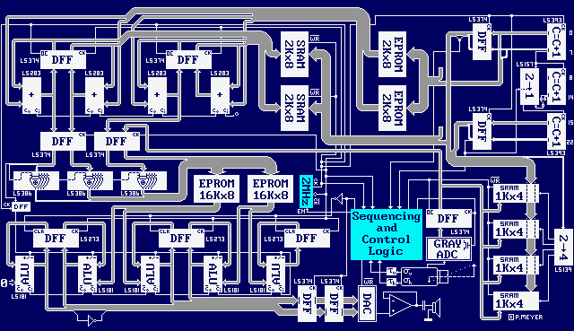
A television frame is scanned by the camera 50 times per second. The scanning takes place from left to right (64us per horizontal line, i.e. 15625Hz), and from top to bottom (312/313 lines). The 625-line standard black&white television signal applies interleaving, alternatingly scanning 312 vertical lines in one 20ms frame and 313 lines in the other. Because we need only a vertical resolution (horizontal to the user) of 64 pixels, we grab one arbitrary 20ms frame to minimize blurred images. The system frequency is independent from the camera frequency, so synchronization is needed for frame grabbing. The frame grabbing process is enabled when bit 21 of the counter CNT1-3 becomes low, which happens when the previous image-to-sound conversion is completed. The system then halts (clock disabled) until a vertical synchronization pulse in the television signal occurs (ADVSNC). Subsequently a monoflop MON adds another 1.52ms delay. This ensures that we skip the top margin of the frame (the left margin to the user, which is also invisible on the monitor). Another monoflop MON is then enabled, and triggered by a horizontal synchronization pulse in the television signal (ADHSNC). This adds another 15.2us delay to skip the left margin of the frame (the bottom margin to the user, also invisible on the monitor). Then the system clock is enabled, allowing the counter to count freely while the first horizontal line (leftmost vertical user line) is scanned. During one clock phase the video signal is sampled in a sample-and-hold stage and converted into Gray-code by a set of comparators. During the other clock phase, when the 4-bit code has stabilized, the resulting digital grey-tone is latched and stored in video memory, while the sample-and- hold stage is opened for capturing the next video sample (pixel). The clock is disabled after 64 clock pulses, i.e. 32us, which covers most of the area visible on the monitor. By then we have stored the first 64 pixels. After a horizontal synchronization pulse and a 15.2us delay from the monoflop the clock is enabled again for the second line, etc. Because of the counter configuration CNT1-3, with CNT2 bypassed, only every fourth line of the television signal causes an increment in the most significant 6 bits addressing the video memory PIX1-4. So only the last of every four lines is actually remembered for later use. The others are overwritten. This is meant to make uniform use of the 312/313 line frame. Effectively grabbing only every fourth line ensures that our 64 vertical pixel resolution covers 64*4=256 lines of the frame, which is almost the whole visible field on the monitor. After 256 scanlines, bit 21 of the counter becomes high, disabling the frame grabbing and restarting the image-to-sound conversion.

16-bit digital to analog converter (DAC) and sample-and-hold circuit

Digital processing

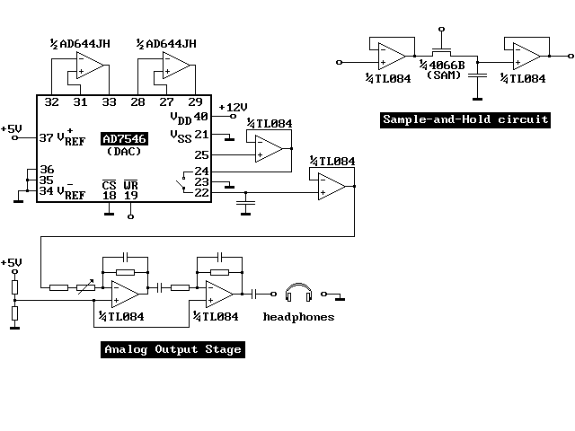
The 2MHz system clock INVCK,DIVCK is driven by an 8MHz cristal. Starting at the upper right corner we find three dual 4-bit binary counters CNT1-3 driven by the system clock. These generate addresses for phase and phase change memories and also for the video memory. The six lsb's of the top counter always indicate a particular oscillator (phase and phase change memory) and its corresponding pixel height (video memory). During image-to-sound conversion, the counters are normally configured as one large 23 bit ripple-carry counter. During frame grabbing, the multiplexer MUX bypasses the 7-bit middle counter to give a 128-fold increase in the frequencies of the most significant counter bits (the bottom counter). This is needed to grab a video frame within the 20ms (50Hz) television single frame time and thus avoid blurred images. The six msb's of the bottom counter always indicate a particular vertical scanline (horizontal position). The middle counter just ensures that it takes some time (and sound samples) before the next vertical scanline is going to be converted into sound. The 2MHz input to the top counter causes the output of the top counter to change every 500ns. During image-to-sound conversion the output of the bottom counter changes every 500ns*2^8*2^7=16.4ms, so the conversion of the whole image, i.e. 64 vertical lines, takes 64*16.4ms=1.05s. For experimental purposes it can be most easily changed into a 2.1 second conversion time by using the full 8 bits of the middle counter, which is the purpose of the switch SW. In that case the counters are configured as one large 24 bit counter. However, in the discussion we will assume a 7 bit middle counter (1.05s conversion time) giving a 23 bit total counter (bit 0 through 22), unless stated otherwise. The addresses generated by the counters go unlatched to the phase change EPROMs DFI1,2 while they are latched by L1CNT,L2CNT before going to the phase SRAMs FI1,2. This is meant to take care of the fact that the EPROMs are much slower (250ns) than the SRAMs (150ns). Therefore the EPROMs receive their addresses 250ns earlier. The phase change of a particular oscillator read from the EPROMs is added to the present phase read from the SRAMs. The summation takes place in the 4-bit full adders AD1-4, and the result is latched by octal latches L1FI,L2FI before being rewritten into the SRAMs. The new phase is also sent down the latches L3FI,L4FI, together with 4 bits pixel brightness information coming from the video SRAMs PIX1-4. After the possible negation (ones complement) by the exclusive- ORs XOR1-3, the phase and brightness are used as the address for the sine EPROMs SIN1,2. These give a sine value belonging to the phase range 0..PI/2 (1st quadrant), and scaled by the brightness value. The whole 2*PI (4 quadrant) phase range is covered by complementing the phase using the exclusive-ORs and by bypassing the sine EPROMs with an extra sign bit (the line passing through the D- flipflop DFF2; this flipflop gives a delay ensuring that the sign bit keeps pace with the rest of the sine bits). The sign bit determines whether the ALUs ALU1-5 add or subtract. The ALUs combine the results of all 64 emulated oscillators in one superposition sample. The latches L1SIN,L2SIN,L3SIN are just for synchronization of the adding process. When the superposition has been obtained after 64 system clock cycles, the result is sent through the latches L1DAC,L2DAC to the 16 bit digital-to-analog converter DAC. The inverter at the bottom of the figure serves to give an offset to the summation process by the ALUs after clearing the latches. The DAC input range is 0000H till FFFFH, so the starting value for the addition and subtraction process should be halfway at 8000H to stay within this range after adding and subtracting 64 scaled sine samples. The present design keeps the superposition almost always within this range without modulo effects (which would occur beyond 0000H and FFFFH), even for bright images. This is of importance, because overflows cause a distracting clicking or cracking noise. The average amplitude of the superposition will grow roughly with the square root of the number of independent oscillators times the average amplitudes of these oscillators. This can be seen from statistical considerations when applying the central limit theorem to the oscillator signals and treating them as stochastic variables, and simplifying to the worst case situation that all oscillators are at their amplitude value (+ or -). Therefore the average amplitude of such a 64 oscillator superposition will be about 8 times the amplitude of an individual oscillator, also assuming equal amplitudes of all oscillators (as in a maximum brightness image). This factor 8 gives a 3 bit shift, which means that we must have provisions for handling at least 3 more bits. This is the purpose of ALU5, which provides 4 extra bits together with part of L3SIN (*). The output of the DAC is sent through an analog output stage, indicated only symbolically by the opamp. Finally the result reaches the headphones.

(*) Numerical calculations on sine superpositions showed that for a very bright image field, 3 bits would cause overflow 16% of the time, whereas 4 bits would cause overflow during 0.5% of the time. Experimentally, this appeared to be still too much. Overflows for large and very bright image parts were heard as a disturbing "cracking" sound. Division of all sine values in the EPROMS by 4 cured the overflow problem with no noticable loss of sound quality (a 16 bit sine value would have been rather redundant anyway).

We have now more or less followed a particular oscillator sample through the system. When the image-to-sound conversion is complete, as indicated by bit 21 of the counter CNT3, the frame grabbing process starts.

The analog video signal from a camera is sent through a sample- and-hold circuit SAM and converted to a 4-bit digital signal in Gray code by ADC1-15. This serves to reduce the probability of getting very inaccurate results due to transition states (spikes and glitches). The 4-bit code is then stored in video SRAM in PIX1-4, which receives its addresses from the counter CNT1-3. 2 bits of this address are used for chip selection by the demultiplexer DMX.

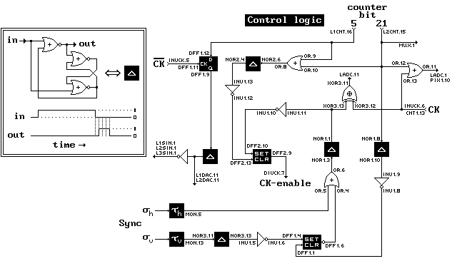
Finally, there is the control logic (or "random" logic) that takes care of the detailed timing, synchronization and mode switching (frame grabbing versus image-to-sound conversion). The meaning of the symbols in the control logic is the following. The tau's represent triggerable delays (monoflops MON). The small sigma's represent the horizontal and vertical synchronization pulses of the television signal, the outputs of the comparators ADHSNC and ADVSNC. The delta's represent differentiating subcircuits that generate a three- gate-delay spike on the trailing edge of an input pulse. This spike is long enough to trigger subsequent circuitry.

Sequencing and control logic

Copyright © 1996 - 2024 Peter B.L. Meijer